Object Tracker with FPGA
The bulk of the content here has been written, but still missing a few images/diagrams.
If there are any clarification questions, feel free to reach out!
TLDR Summary
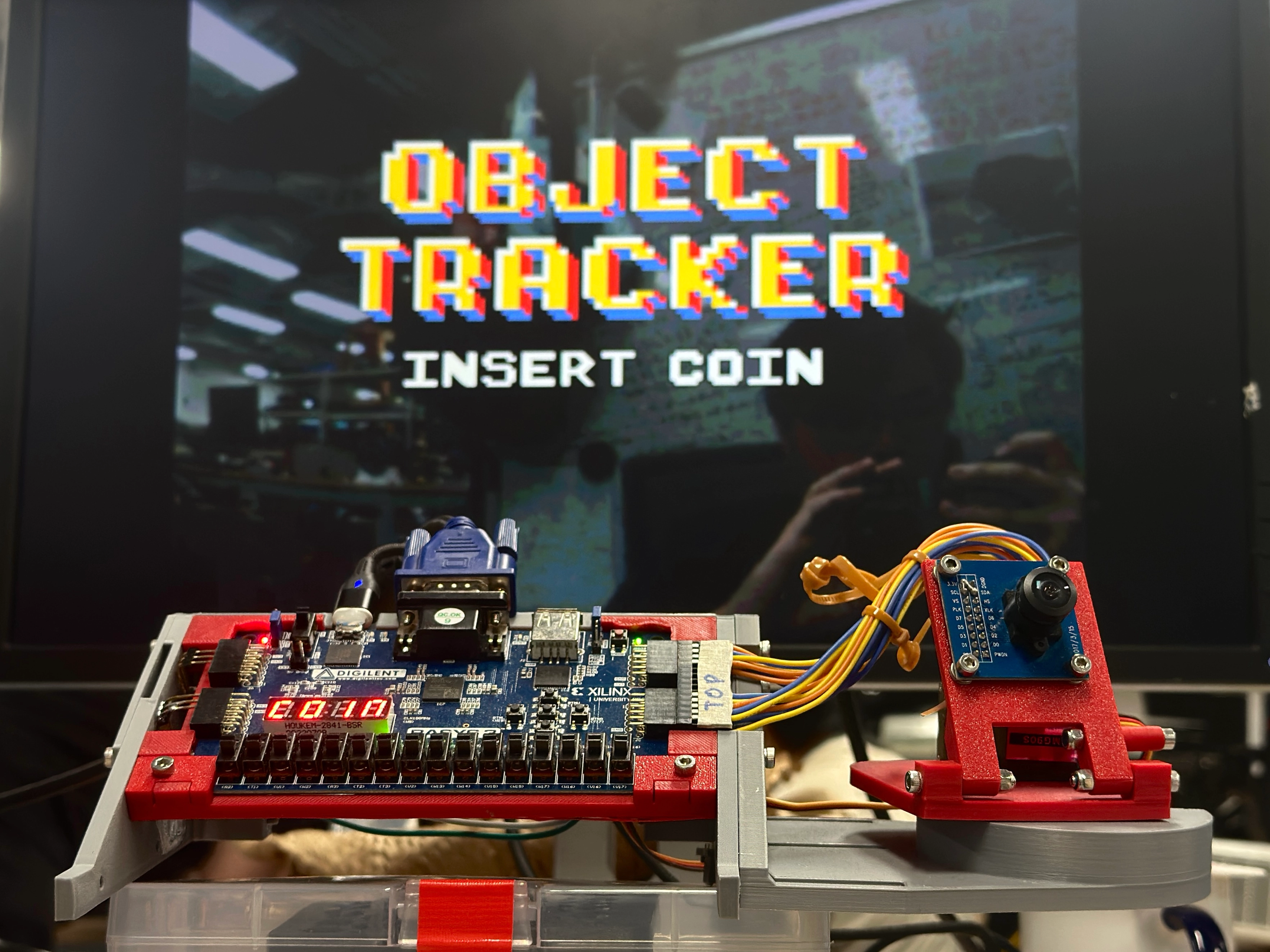
Developed an object tracking system with a GUI for a fully customisable computer vision pipeline, all implemented on a single Basys3 FPGA board.
Video Demo
Introduction
“eh why every EE project end up tuning PID ah?”
This was the final project for EE2026: Digital Design. This module is an introductory digital logic course, with a strong emphasis on the practical aspects of implementing digital systems on FPGAs using Verilog.
The final project was completely open-ended, with the only restriction being that only a single bitstream can be used with up to 4 FPGA boards (Basys3 FPGA Board).
The typical projects implemented are recreations of popular games or enhanced versions of the suggested project, which was a graphing calculator. However, given that this was essentially the only module in our course that allowed for a fully open-ended project, we decided to push the limits of what could be done with this simple FPGA board. There were two key considerations:
- The project should exploit the features of the FPGA e.g. high level of parallelism, low and deterministic latency, etc. In other words, it should not be something that could be easily done with a standard microcontroller or CPU.
- The final result should be a product, i.e. a cohesively designed system that has a clear function, rather than a haphazard collection of boards and wires.
Ultimately, we landed on an educational tool for teaching basic computer vision (CV) concepts. This was done by implementing a GUI, displayed on a VGA monitor, that allowed users to customise an image processing pipeline for colour-based object tracking using simple drag-and-drop blocks. The camera was also mounted on a pan-tilt assembly with tunable PD controllers to physically track the object in real-time.
This project met all of our requirements: image processing operations ran in parallel with fast, predictable memory access times to allow for real-time performance, while the GUI and pan-tilt assembly made for a fun and interactive product.
The sections below detail the various components of the project, while also explaining the design choices we had to make along the way, in a (somewhat) chronological order.
CV Pipeline
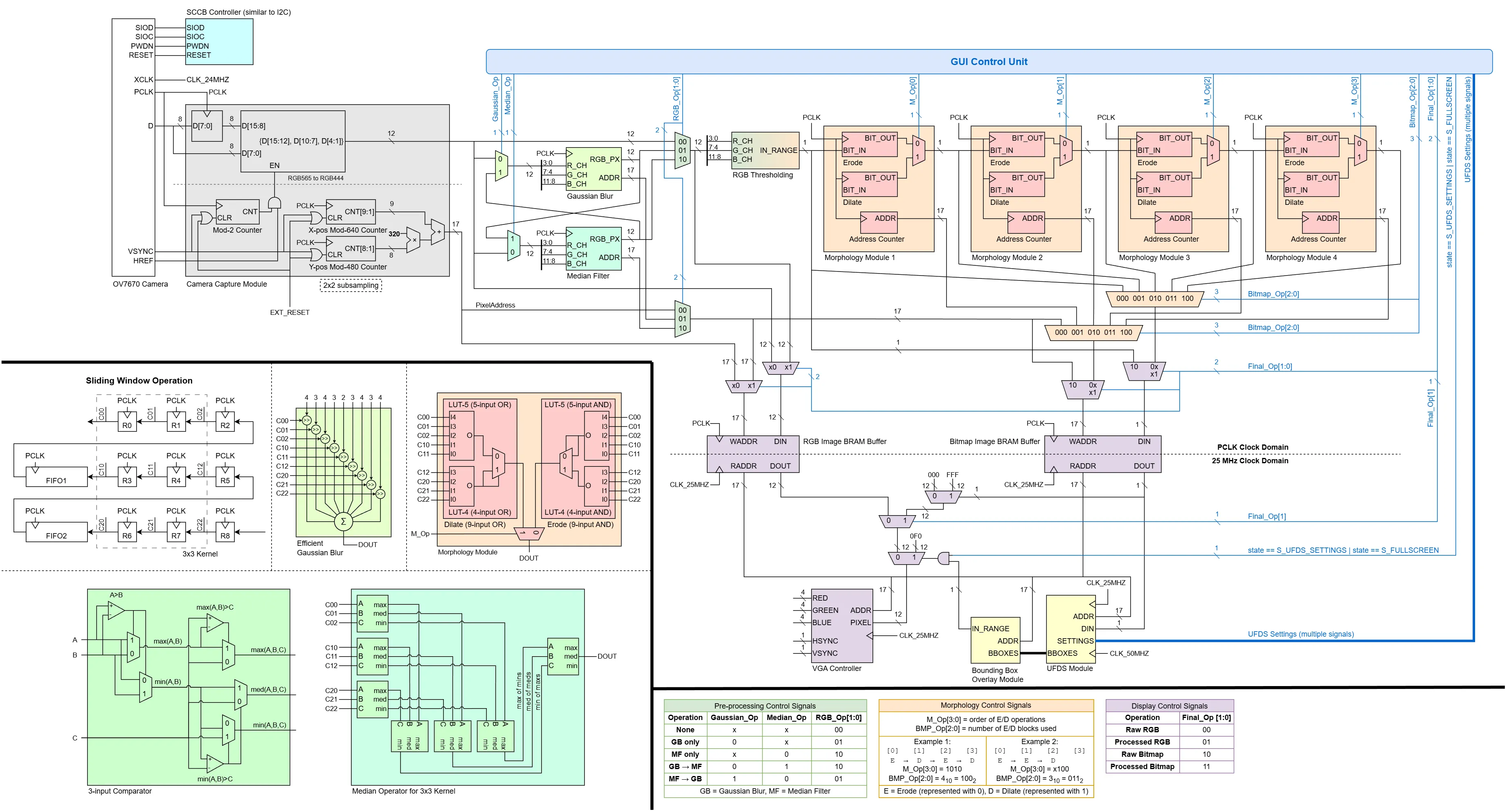
The overall architecture of the CV pipeline is shown below. Broadly speaking, the pipeline can be divided into 5 main stages:
- Camera Interfacing (Grey): Configuring the camera’s settings, and reading the pixel data from the camera.
- Pre-Processing (Green): Blurring the image to reduce noise.
- Thresholding and Morphology (Orange): Thresholding the image based on colour ranges to create a binary bitmask, which undergo erode/dilate operations to clean up noise.
- Blob Detection (Yellow): Finding contiguous regions in the bitmask i.e. finding objects.
- Buffering and Display (Purple): Saving the processed image into BRAM buffers and rendering them on the VGA display.
In addition, user settings from the GUI (Blue) are decoded into control signals that modify the datapath accordingly, as summarised in the tables at the bottom.
Camera Interfacing
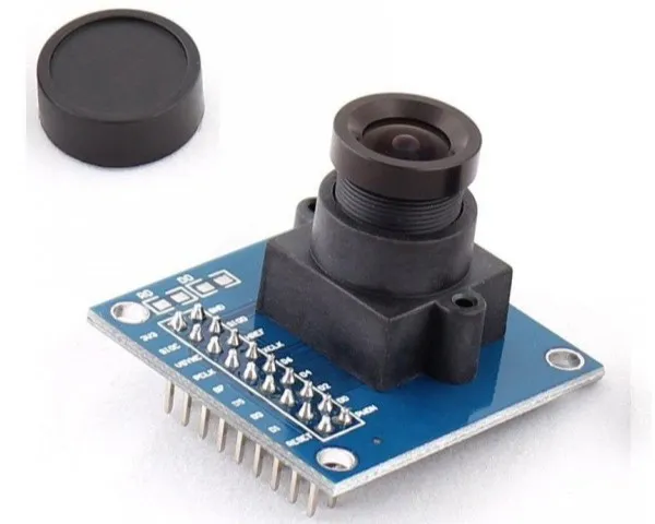
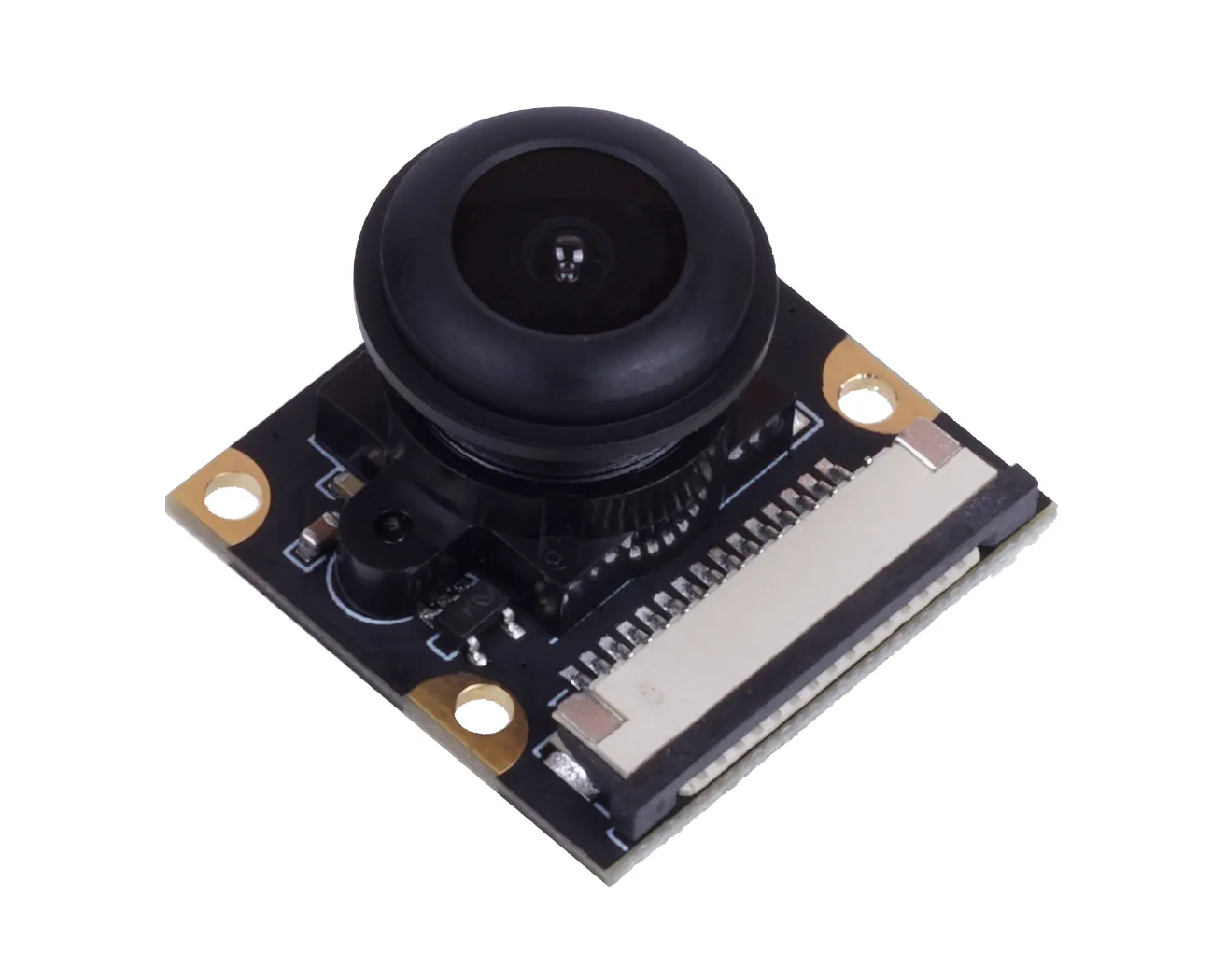
The camera used was the OV7670 Camera Module. This is a low-cost camera module that had been used in many existing FPGA projects that inspired us to embark on CV in the first place, e.g. Camera Display to VGA, Edge Filter, Stereo Vision. The original lens was swapped out for a wider 130 degree FOV lens taken from a Seeedstudio camera module.
To interface with the camera, the SCCB protocol is used to set up the camera’s registers, which configures the camera’s operating parameters e.g. resolution, colour format, sensor gain, etc. This protocol can be regarded as a proprietary variant of I2C, since writing of data follows a “3-Phase Write Transmission Cycle”, which is essentially the same as I2C’s structure of procedurally sending the (1) device address, (2) sub-address, (3) data byte, all at a 100 kHZ clock.
The actual implementation can be understood as a series of finite state machines (FSMs). On initial start-up, a register array stores a list of concatenated 8-bit configuration register addresses with their corresponding 8-bit data bytes. A counter is used to send these values to the SCCB controller sub-machine sequentially.
The SCCB controller packs these values into a shift register with the correct message format by adding start/stop condition bits and the camera address. A separate shift register also keeps track of the progress of the transmission, which lets the controller know when to drive the data line to high impedance to read the ACK/NACK response from the camera. Once this status shift register is cleared, the signal indicating active transmission is cleared, which increments the register array counter in the FSM and starts a new message.
Odd quirks: A dumb issue encountered was that after writing the first byte (0x80) to the COM7 register (0x12), which is supposed to reset all other registers, a “pause” had to be inserted by writing a default value to some register, before proceeding to write the rest of the configuration registers. Not doing so resulted in our next immediate register write (which was meant to set the image size and pixel format) to be ignored, causing the pixel capture module to output garbage pixels.
Once the camera is configured, pixel data is streamed in the chosen format (RGB565) over an 8-bit parallel data bus synced to a pixel clock (PCLK) generated by the camera. Synchronisation signals similar to VGA are also provided to indicate frame ends (VSYNC) and line ends (HREF).
Each RGB565 pixel is sent over 2 bytes, with the first byte and second byte containing the upper and lower 8 bits respectively. (Image Source: Omnivision Technologies)
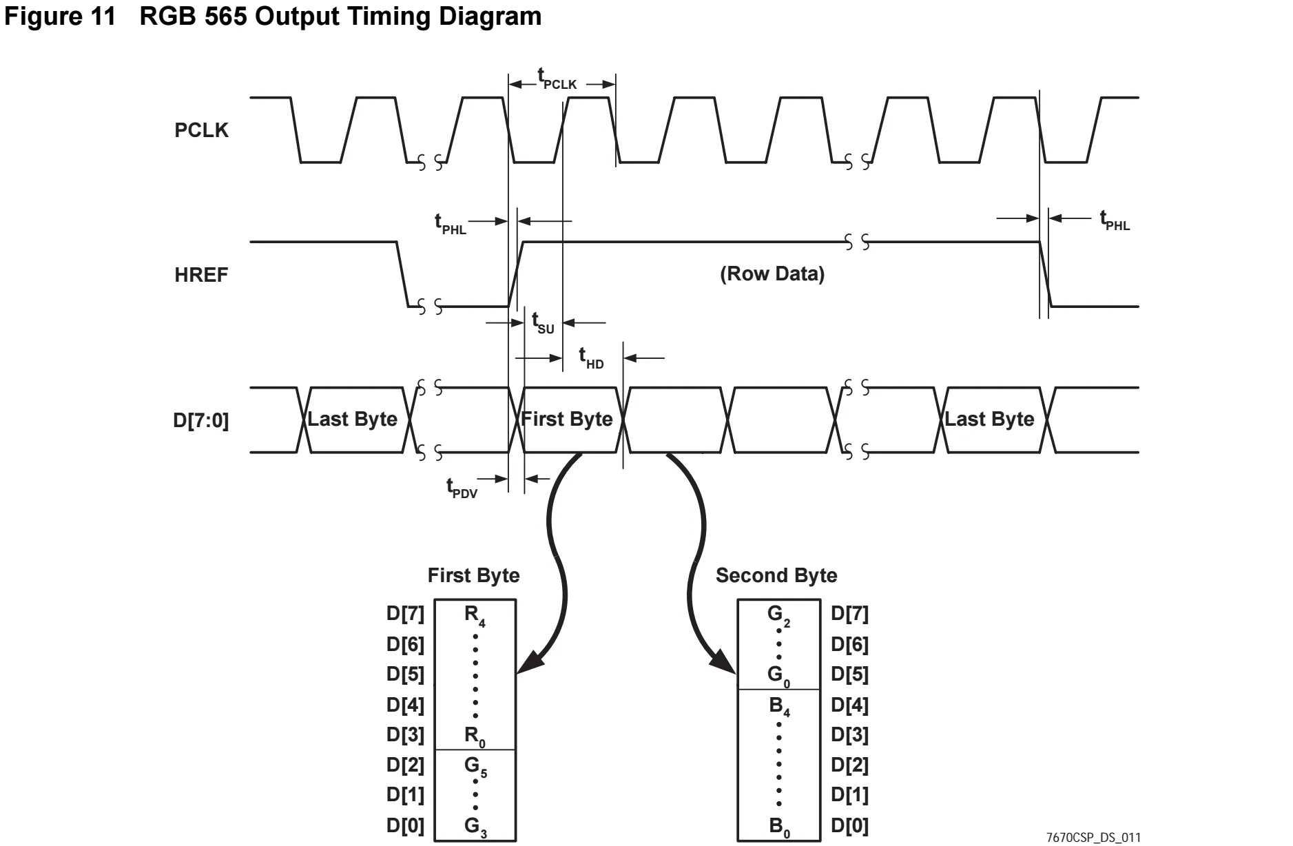
The Capture module is responsible for reconstructing the pixels from this byte stream by buffering the first and second byte into a 16 bit register. Due to memory limits, the image is downsampled into RGB444 format by truncating the least significant bits of each colour channel, and this 12-bit pixel is output on every 2nd PCLK rising edge.
Simultaneously, a row and column counter is maintained to keep track of the pixel’s position in the frame, which is also reset upon VSYNC/HREF signals to ensure synchonicity. Due to the same memory limits, the image is also downscaled from the camera’s 640x480 resolution to 320x240 by only capturing the 2nd pixel in both dimensions. Hence, the least significant bit of both row and column counters are ignored before calculating the pixel’s address, which is simply given by . This address directly represents the BRAM address where the pixel will be stored.
Actually, the OV7670 camera has a built-in downsampling feature to output both QVGA and RGB444 directly, but I could not get it to work for some reason (likely some byte alignment or timing issue). However, since there was limited time plus no credit would have been given for interfacing with external peripherals, I did not bother debugging further as manual downsampling was already implemented.
Sliding Window
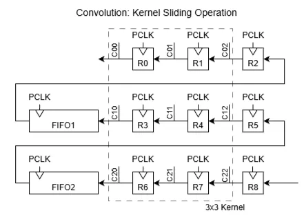
All the image processing operations used (both in pre-processing and morphology stages) fundamentally rely on the sliding window, just with different kernel operations. This is implemented most efficiently with shift registers to store the values in the kernel, while FIFO buffers store the remaining rows of pixels, where is the height of the kernel. Due to both LUT and BRAM constraints, all operations were limited to a 3x3 kernel. (GIF Image Source: TowardsAI)
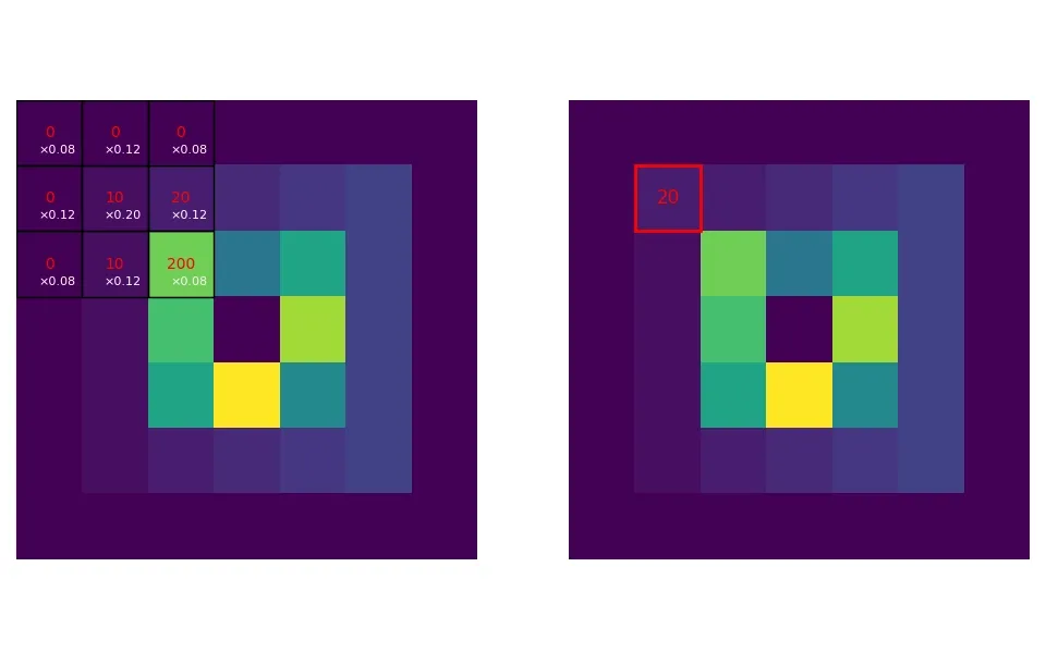
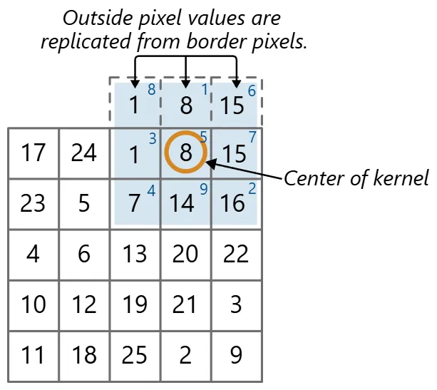
However, there are two issues to address for sliding windows, namely border handling and latency. At the borders of the image, there are not enough pixels to fill the kernel. To handle this, we can either ignore the border pixels, which shrinks the output image size by one pixel on each side, or use padding methods to fill in the missing values.
Padding was chosen to keep the image size consistent throughout the pipeline. Replication was used for pre-processing operations (i.e. RGB images), while min-/max-padding was used for morphology operations (i.e. binary bitmasks). (Image Source: Mathworks)
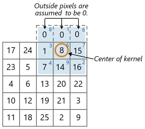
The other issue is latency from stacking multiple sliding window operations. At the start of a frame, the operation needs to wait for the first row of the image to fill the top 2 rows of the kernel and FIFO buffers (using either replicate or min/max padding for the top row), as well as the second row first 3 pixels fills the last row of the kernel. That is when the kernel is fully filled and thus the first kernel operation can be performed. The same issue persists for each subsequent sliding window stage, resulting in a latency of one row plus one pixel introduced for every new stage.
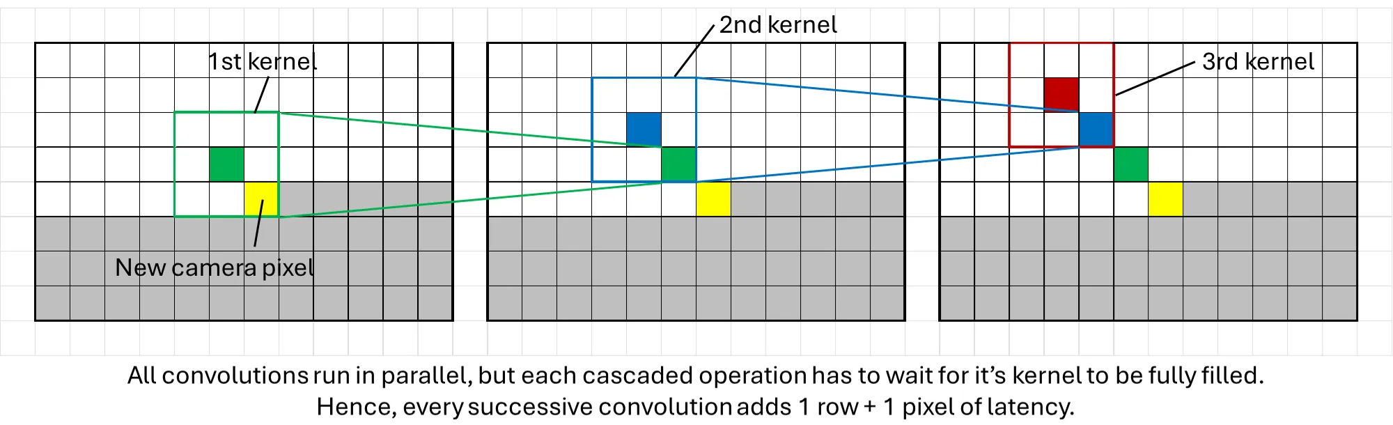
This becomes an issue at the end of the frame, where each convolution stage is still processing the last few rows of the image while the next frame has already started streaming in. The proper way to fix this would be to implement an additional one-line buffer for each stage that reads the next frame’s pixels until all the previous frame’s pixels have been processed with the existing sliding window.
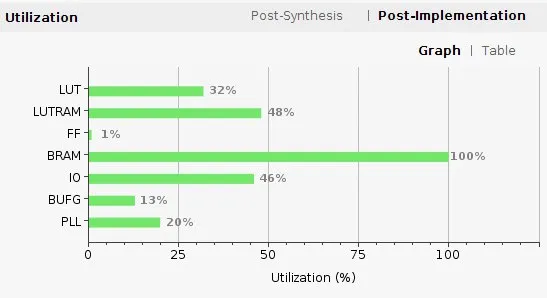
However, this would have increased BRAM usage (which eventually reached 100% utilisation). Hence, a simpler solution was used instead: simply ignore the last few rows of the image that was not processed. This was acceptable since the GUI blocked the bottom part of the frame anyways and a few rows of pixels made little difference to the overall user experience.
Kernel Operations
With the sliding window in place, implementing the various kernel operations was rather straightforward. The main restriction was that all operations had to be completed within a single clock cycle to ensure no further latency was introduced.
For RGB images, each individual colour channel was processed separately in parallel, then recombined back into a RGB pixel, which is valid for linear filters like gaussian blur. For non-linear filters like the median filter, the proper way would be to find the pixel with the smallest sum of squared differences across all 3 colour channels, compared with every other pixel in the kernel. Alternatively, the pixels could be converted to another colour space like HSV where performing median filtering on each separate channel makes sense.
However, both methods added computationally expensive operations that were deemed infeasible to run in a single clock cycle. Hence, the median filter was applied to each individual colour channel instead. Colour inaccuracies produced were deemed acceptable since each colour channel is only a 4-bit value, so accuracy was not a major concern.
For the actual implementation in hardware, the gaussian blur is simply a multiply-and-accumulate operation between the image kernel and a separate fixed kernel. This was further simplified by approximating the kernel values to their closest powers of 2, allowing for efficient implementation using bit shifts only.
The median filter was inspired from this paper. A 3-input comparator block is first made using a minimal number of comparators and multiplexers, which outputs the maximum, median and minimum of 3 input numbers. Then,
- The 9 values in the kernel are first passed through a layer of comparators in groups of 3, where the max, median and min are grouped together as inputs for a second layer of comparators.
- Then, the lowest value from the maximum group, the middle value from the median group, and the highest value from the minimum group are fed into a final comparator.
- Finally, the median value of this final comparator becomes the median of the 9 numbers.
This method of deriving the median is more efficient as it uses less comparisons than the typical sorting network approach. The block diagrams below explain what the gaussian blur and median filter look like in hardware.
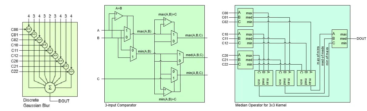
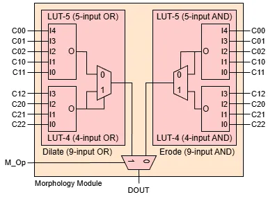
Finally, the erode and dilate operations for binary images were simply a bitwise and/or of all pixels in the kernel respectively. Both operations were combined into a single module, with a final multiplexer determining which operation is applied to the output.
Colour Thresholding
To determine regions of interest in the image, basic colour thresholding was implemented. As the final image streamed to the VGA display is in RGB format, thresholding was also done in RGB colour space for convenience. If a pixel’s Red, Green and Blue channels fall within the user-defined ranges, then it is assigned a value of 1 in the converted bitmap, else it’s a 0.
Admittedly, thresholding in another colour space like HSV would have been more intuitive and we did consider doing that but there were simply more urgent features to implement at the time. To help with this, an eyedropper tool was added to the GUI, which allowed the user to simply click on any point in the image to sample it’s RGB value. This is explained in more detail in the GUI section below.
Memory Management
The Basys3 board only has 1.8 Mbits of BRAM available with no other external memory. For reference storing a single 320 by 240 px, RGB444 (12 bit) image is already 0.92 MB, just above half the available memory.
To further complicate things, the camera feed is streamed to the VGA display at 60 Hz while the camera feed is incoming at 30 FPS, which means that one full frame must be held in memory for the VGA output while the next frame is being processed. Initially, a double buffer was used by cutting some of the left-most pixels, storing two 310 by 240 px frame buffers that used up 100% of the BRAM.
However, once we started work for the GUI, more BRAM had to be freed to store those elements. An attempt was made to create a “1.51” times buffer (think of it as three half-frame rolling buffers with a little extra buffer space).
The diagram and explanation below describes the theory of operation with a 1.6x buffer:
- Let each column represent a snapshot in time of how the BRAM is filled.
- Let each box in a column of BRAM represent one-tenth of an image (i.e. an image chunk). Since this is a 1.6x buffer, there are 16 boxes per column.
- Let the time interval between each snapshot be one-tenth of 1/60 seconds, i.e. the duration it takes for the 60 Hz VGA display to show 1 image chunk.
- Since the camera frames are incoming at a slower 30 Hz, a new image chunk is filled once every 2 columns (intervals of 1/30 seconds).
- For illustration, let the first frame fill the first 10 chunks of the buffer i.e. the yellow blocks (ignore VGA output for now).
- For the next incoming frame, when half of it is in the buffer (green blocks), the VGA display would have finished showing the old frame once (orange outline in the yellow blocks).
- Then, when the VGA display starts showing the old frame the second time, the new frame will continue writing into the excess buffer space (block number 6 with red outline in the green blocks).
- Once the excess buffer is filled, the new frame loops around and starts overwriting the old frame (blocks 7-10 with red outline in the green blocks). However, since the VGA display output already had a headstart and runs at a higher frame rate, the old frame still displays correctly (remaining orange outlined yellow blocks).
- Once the new frame is fully written (green blocks), the VGA display now jumps to displaying it (orange outlined green blocks). The new frame gets written (blue blocks), and the cycle repeats.
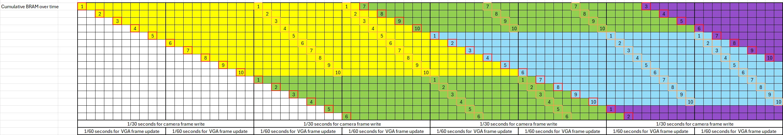
However, we were just unable to get the offset for this rolling buffer to work correctly and had limited time to continue troubleshooting. Plus, our rough calculations showed that even the memory savings from half a frame was likely going to be insufficient to store all our GUI elements.
Hence, ultimately only a single image buffer was used i.e. reading and writing to the same buffer. In theory, this should have resulted in frame tears whenever the frame reader overtakes the frame writer. However, in practice, we found that the frame rate of 30 FPS was high enough to mask these artifacts, plus the image itself is quite low resolution to begin with, so frame defects were essentially unnoticeable.
At one point, we did consider using two FPGAs to overcome the memory limitations. Although the project only permitted using one bitstream even if multiple FPGAs were used, since the BRAM could be initialised with a set of values, an external switch could determine if it simply functions as extra static memory or as a main board.
However, this meant data had to be transferred through external wires at the same rate as the VGA’s pixel clock which is 25 MHz, way above what the FPGA is capable of driving for external signals. Hence, we stuck to the single buffer approach.
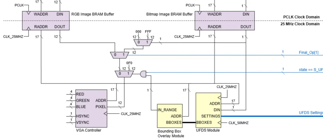
Finally, we wanted the GUI to be able to display both the RGB camera feed as well as the bounding boxes. However, the bounding boxes are calculated from the bitmap image, not the RGB image. Hence, an extra bitmap image buffer had to be included so that it could directly feed into the downstream blob detection module and generate bounding boxes, even when the bitmap is not the image being displayed.
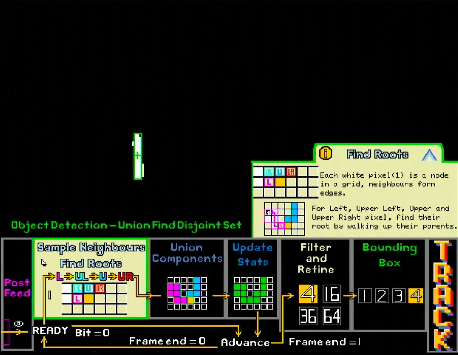
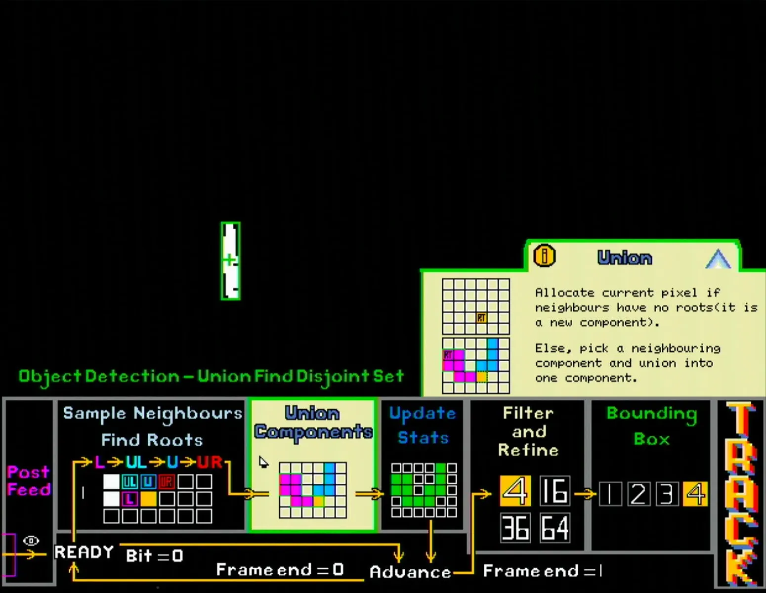
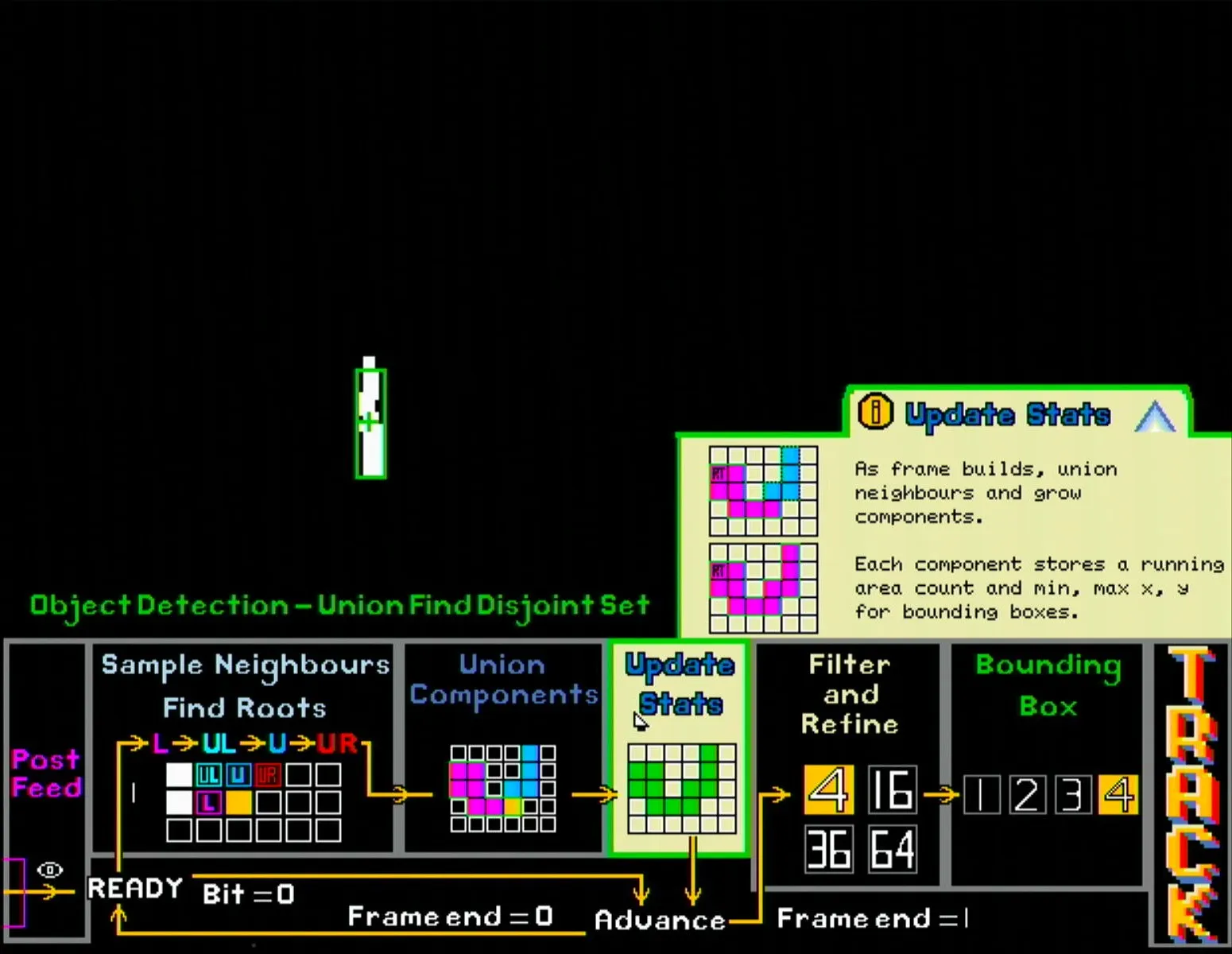
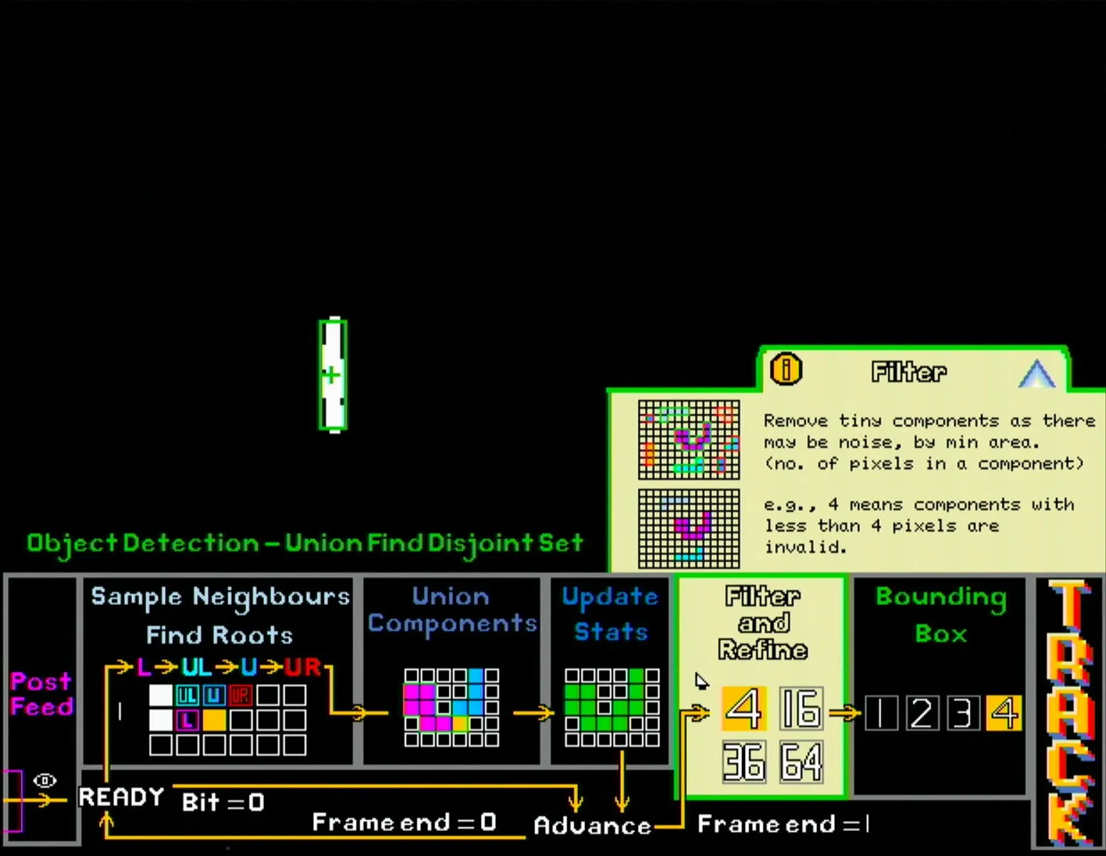
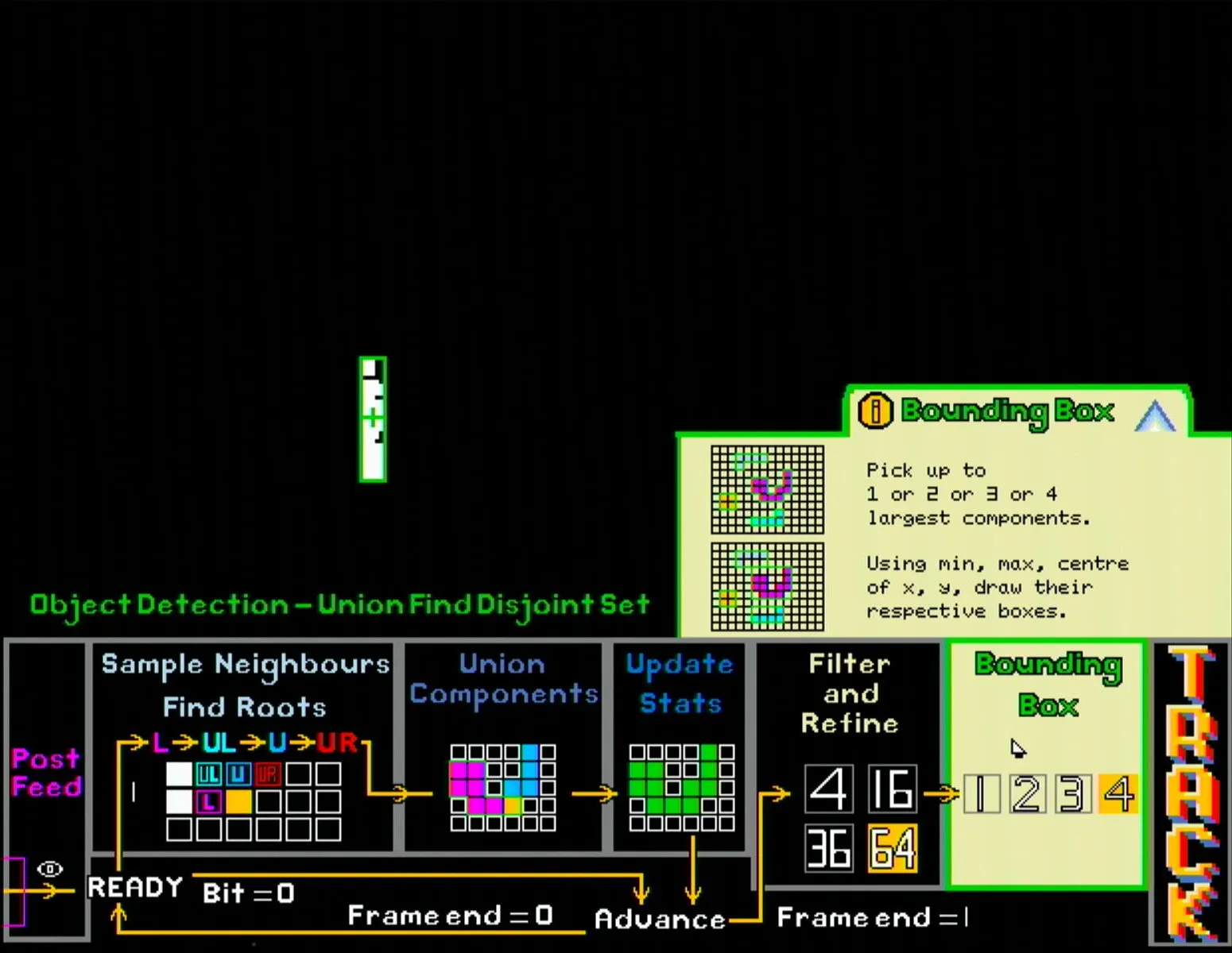
Blob Detection (UFDS)
If we were to draw parallels to the popular OpenCV library, this step would be applying the findContours method on an FPGA. OpenCV’s implementation uses the Suzuki algorithm, which essentially “walks the perimeter” of regions of interest, requiring an entire image frame to do its processing. However, given our requirement for minimal latency, as well as memory restrictions (image is being read and written into the same buffer simultaneously), this algorithm was not feasible.
Instead, a modified UFDS algorithm was used.
- A small 2-line buffer stores the current and previous row of bitmap pixels.
- Each incoming pixel is compared to its 4 adjacent pixels (left, top left, top, top right) to determine if it belongs to a connected component
- A separate set of registers stores min & max XY coordinates and size of all connected components.
- Upon completion of a full frame read, the details of the 4 largest components is piped out to the display module for bounding boxes to be drawn.
All this operates as a state machine running in parallel with the frame capture module but at a higher clock speed, thus ensuring that the component data is immediately available once the new frame is stored, effectively achieving zero latency.
This section is explained in much greater detail by my teammate here.
GUI Design
The overall concept for the user interface is to serve as an educational tool for users to learn about traditional CV methods without code. Hence, the GUI was designed to be as intuitive and interactive as possible.
The screenshots and descriptions below illustrates the typical user journey through the GUI.
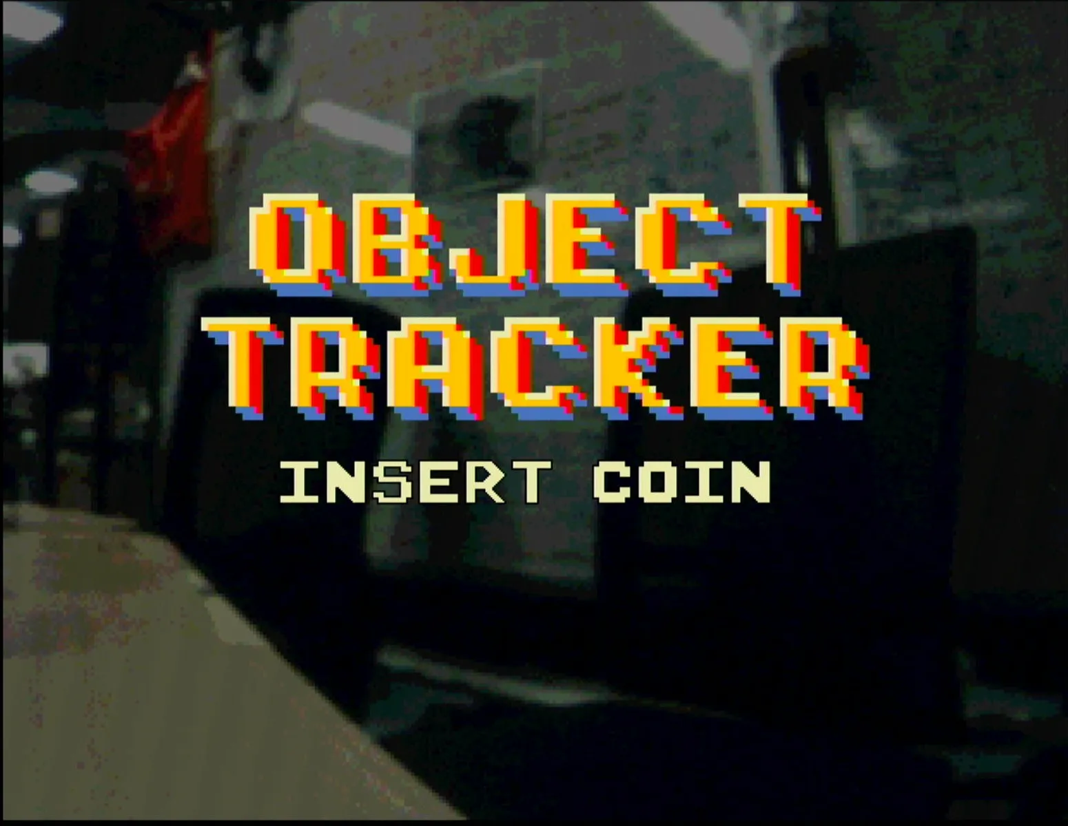
The initial state features a retro inspired title card. The pan servo sweeps back and forth, while the background shows a dimmed version of the live camera feed, thus providing a dynamic background to the splash screen. The user can either insert a coin into the coin slot or click any mouse button to start.
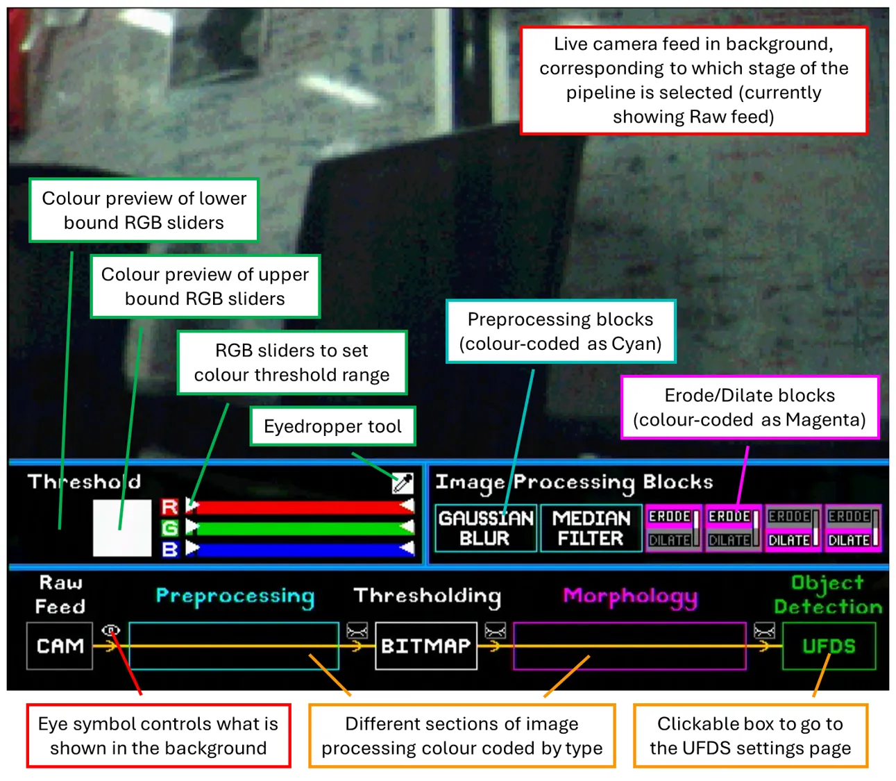
The first screen the user sees is the image processing page. There are 3 main sections: Thresholding, Image processing blocks, and the CV pipeline itself, as shown in the labelled screenshot below.
- Thresholding: Control the colour range used to generate the binary bitmap.
- Sliders: Two sets, one for the lower bound and one for the upper bound, setting the threshold ranges for the RGB channels individually.
- Coloured squares: Previews the actual RGB colour defined by the lower and upper bound sliders.
- Eyedropper: Click once to activate it, then click on the desired pixel in the live feed to sample its RGB values and mark them on the sliders. Users can then adjust the threshold tolerances around those markers.
- Image processing blocks: Blocks that can be drag-and-dropped onto the CV pipeline to change the image filters applied.
- Preprocessing blocks and morphological (erode/dilate) blocks are colour coded and can only be placed in their corresponding sections of the pipeline.
- Morphological blocks can be swapped between erode and dilate functions by scrolling up/down while hovering over the block.
- CV pipeline: Visual representation of the actual image processing steps applied.
- Eye symbols can be clicked on to show the camera feed at 4 different stages of the pipeline: raw RGB image, pre-processed RGB image (blurred), thresholded binary bitmap, and final bitmap after morphological operations.
- Blocks placed onto the pipeline automatically snap and centre themselves into place, as well as update the datapath to provide real-time updates to the camera feed.
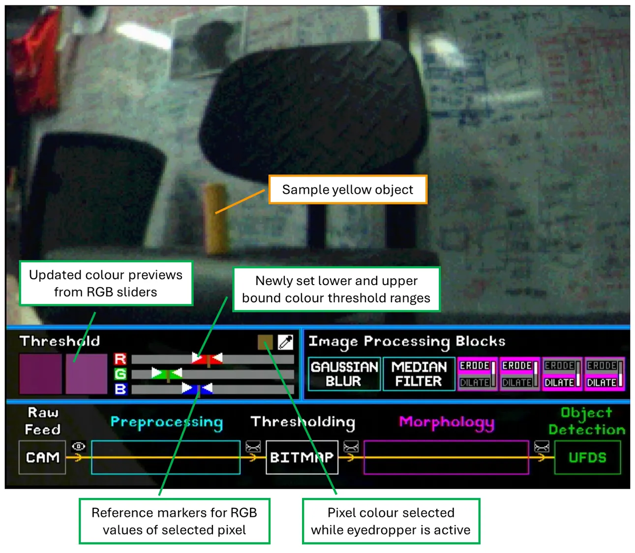
For demonstration, a sample yellow object is used for tracking. As shown below, the selected pixel colour and RGB reference markers show up once the object’s pixel is selected.
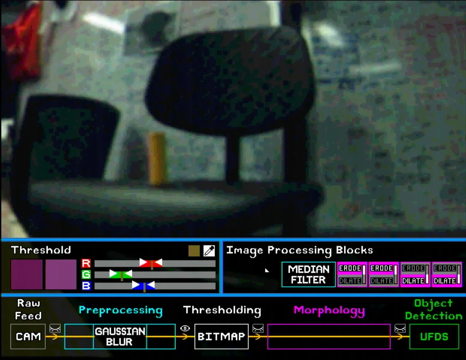
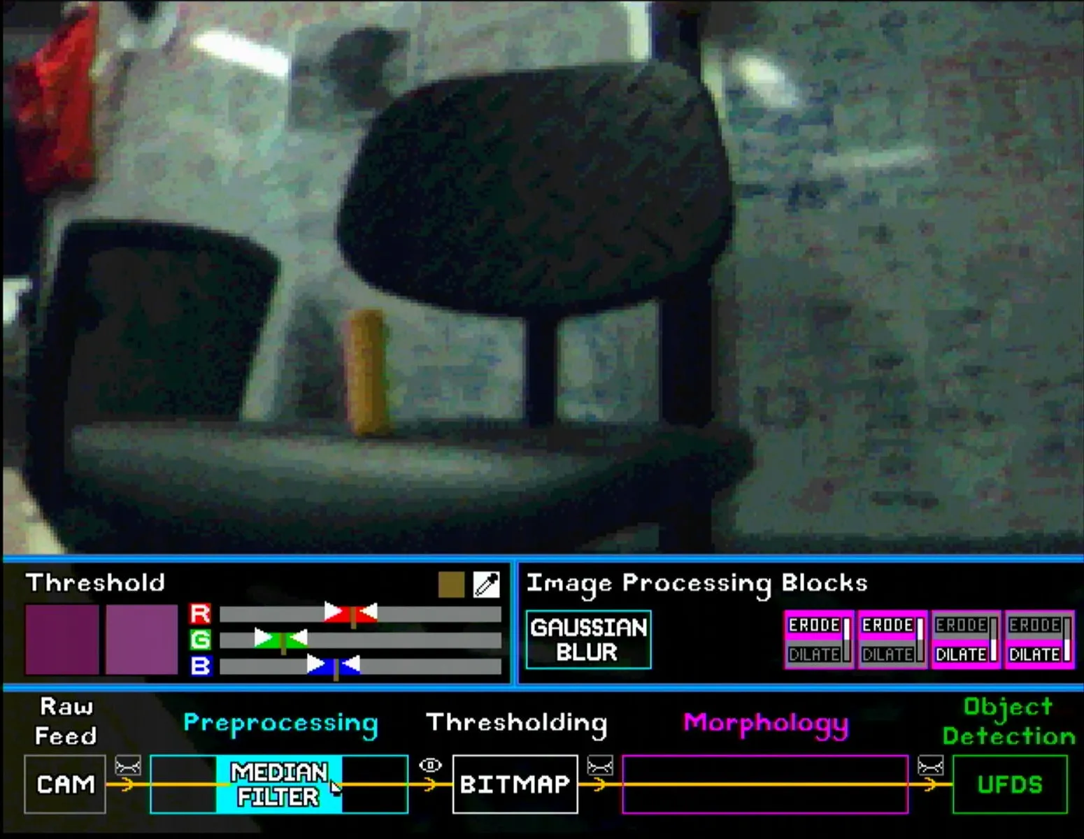
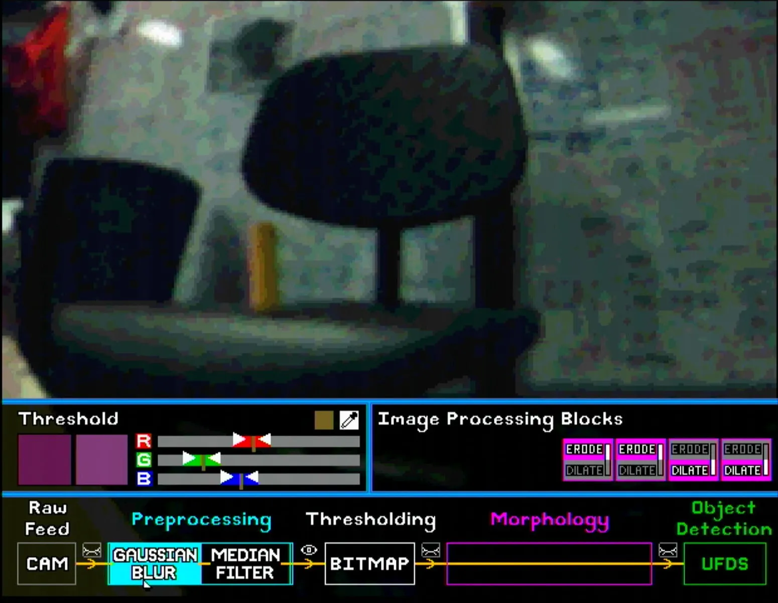
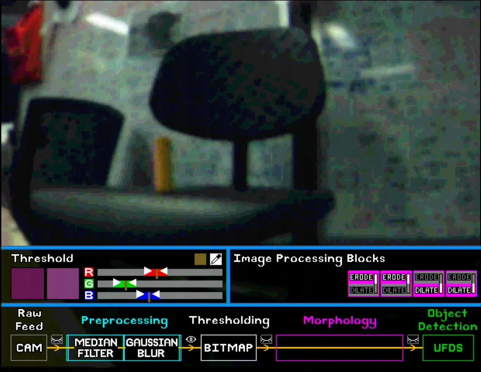
For pre-processing, the user can place the Gaussian Blur and Median Filter blocks in any order. The images below show the subtle differences between different pairings. Note that the eye symbol after the pre-processing section is selected so that the effect of each block is visible.
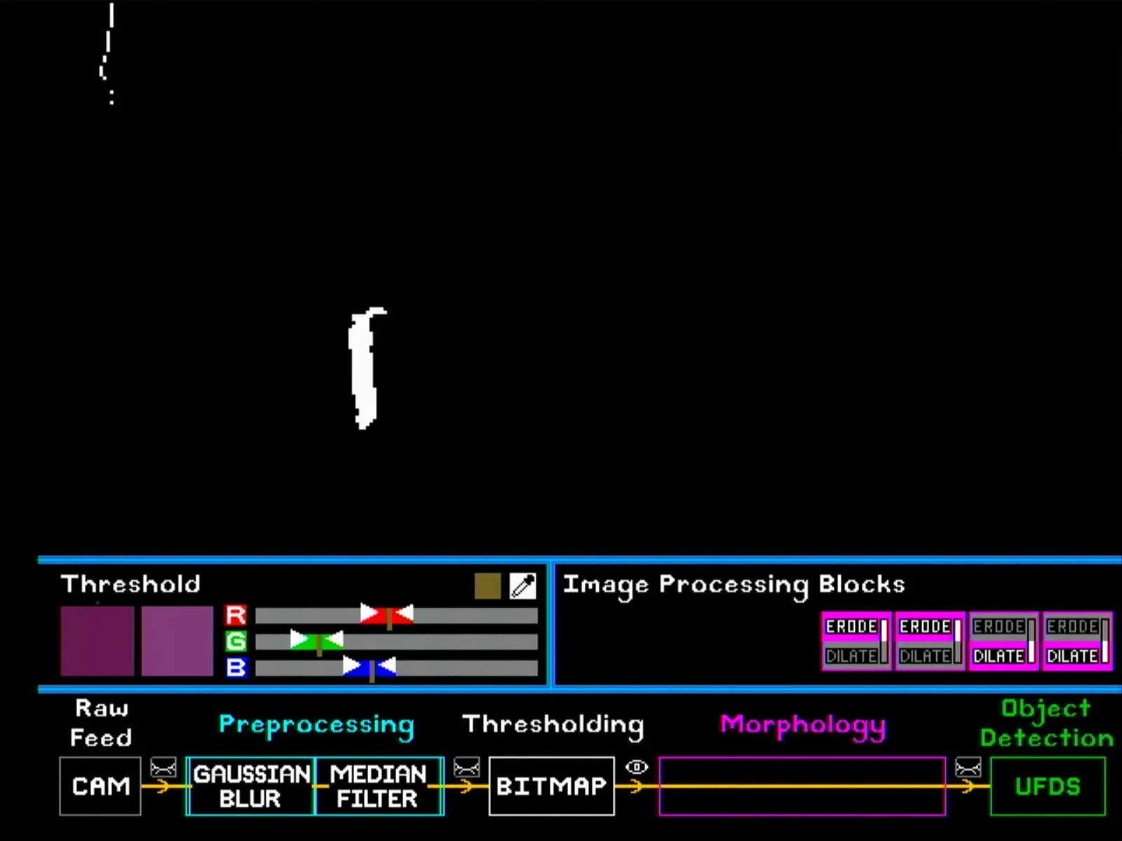
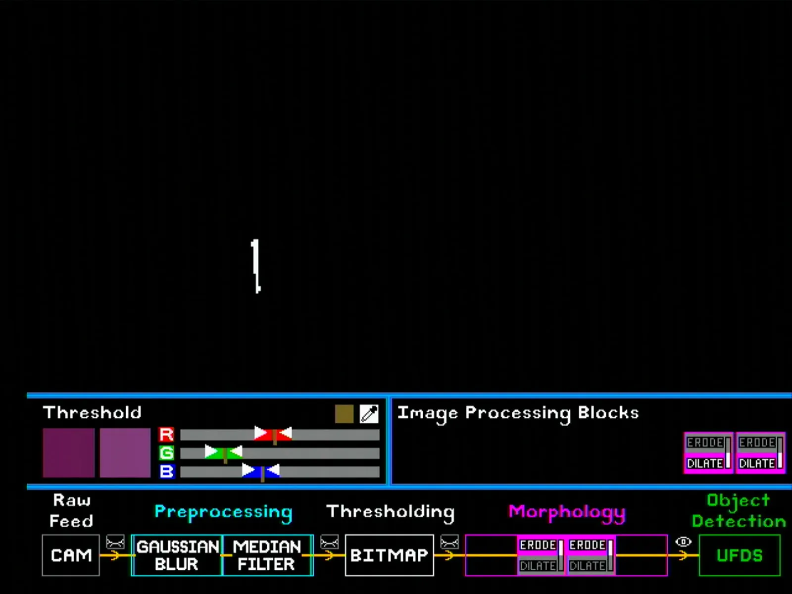
Similarly, for morphology blocks, the user can put up to 4 blocks in any order. Note once again that the eye symbol after the morphology section has to be selected to show the final bitmap. Some configurations are shown below (note the shrinking and enlarging effect of erode and dilate blocks respectively).

TODO: get more screenshots for erode/dilate configurations
Once the user is satisfied with the image processing configurations, they can click the UFDS button to go to the next page for blob detection, which has the following main sections:
- UFDS simplified state diagram
- Shows the main steps of the UFDS algorithm with diagrams.
- UFDS settings
- Filter and refine section allows user to set the minimum amount of pixels needed to be considered as a connected component (i.e. blob). Setting a higher number reduces the chance of noisy pixels being regarded as an object, but also reduces the maximum distance the object can be to remain detected.
- The bounding box section sets the maximum number of bounding boxes to be detected.
- Track button: Activates the pan and tilt servos to start tracking the largest detected blob.
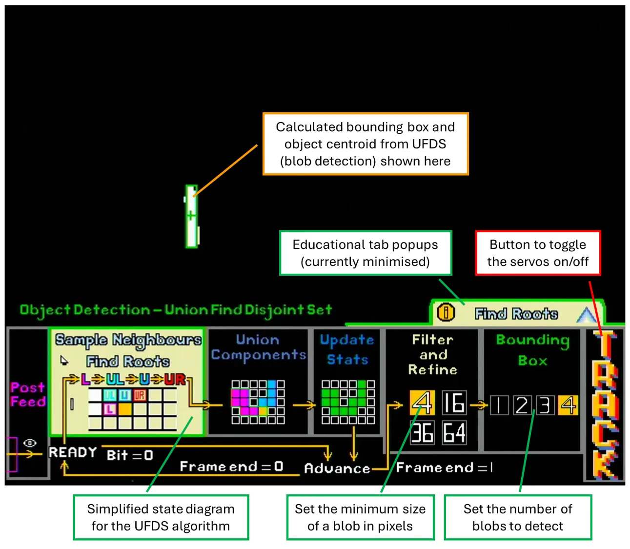
Additionally, the educational pop-ups can be clicked to expand into more detailed explanations and diagrams. Due to the larger amount of text in these pop-ups, all text here is dynamically generated from a fixed alphabet in BRAM, which helped save BRAM at the expense of higher LUT usage (a reasonable trade-off given our resource utilisation).
TODO: get screenshot of educational tab minimised
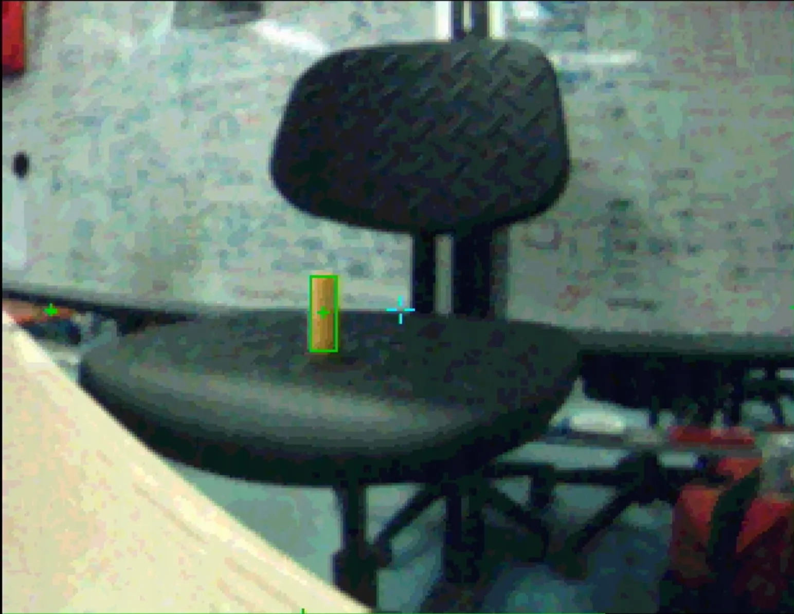
Finally, once all tuning is completed, the user can right click at any page to enter the fullscreen mode. This mode hides all the UI elements, keeping only the bounding boxes and object centroids. It also includes a crosshair in the centre of the frame, which is useful for qualitatively evaluating the tuned object tracker.
The user can choose to enter fullscreen mode with the bitmap, or go back to the image processing page, set the view to the raw camera feed, then enter fullscreen mode with the RGB image showing.
Overall Datapath and Control
Inspired from CPU microarchitecture diagrams, the processing blocks are connected through multiplexers whose outputs are determined by control signals sent from the GUI module.
On the pre-processing side (green), the input to each filter can either be the raw camera feed or the output of the other filter block. The control signals Gaussian_Op and Median_Op are determined by the order of the pre-processing blocks placed in the pipeline, while the output signal RGB_Op is determined by the last operation in the pre-processing pipeline.
For the morphology side (orange), the process is even simpler as the output of each erode/dilate block directly connects to the input of the next block. Therefore, the 4-bit M_Op signal is simply the concatenation of the operations in the morphology pipeline (where erode is 0 and dilate is 1), while the output signal Bitmap_Op is again determined by the last operation, which in this case is just the number of morphological blocks.
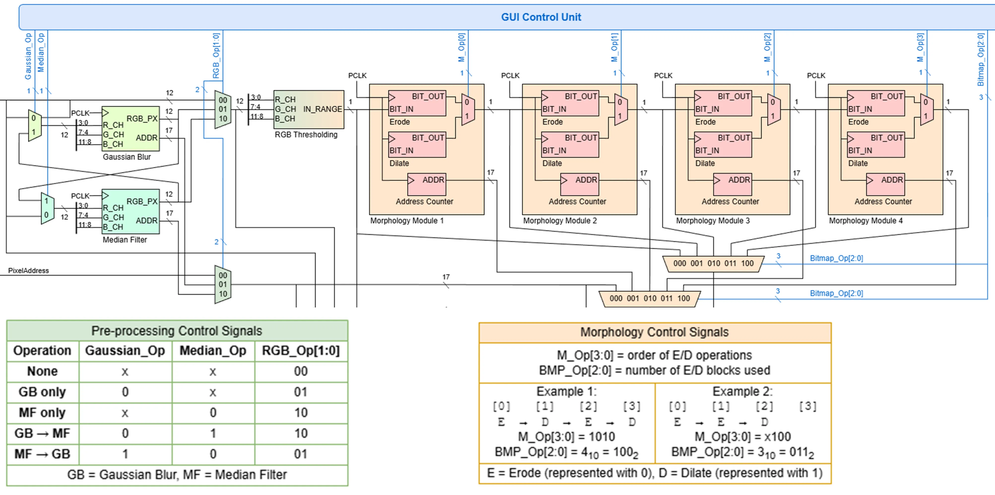
The final displayed output is determined by the Final_Op signal, and this simply comes from which view has been selected in the GUI.
Servo PD Controller
Finally, for users to see a tangible result from their object tracking system, the camera is mounted onto a pan-tilt mechanism. When activated, the servos, running their individual PD control loops, will try to centre the object relative to the camera’s frame, thus creating a physical object tracking system.
The PD controller itself takes the object’s X and Y offset from the frame’s centre as the errors for the pan and tilt servos respectively. Since the servos use position control as input, the calculated PID term is integrated before being mapped to the standard pulse width expected by the servo.
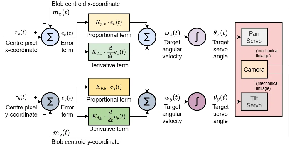
As for tuning of the Kp and Kd constants, pre-tuned values are loaded when initially activated, which are displayed on the seven-segment display as four 4-bit values (pan Kp, pan Kd, tilt Kp, tilt Kd). These values can be modified by pressing btnD, which now continuously assigns the state of the 16 switches on the board to the four 4-bit values. Flipping the switches now changes the Kp and Kd values, providing the user immediate feedback on what changing each constant does. Pressing btnD again exits the editing state and locks in the new Kp and Kd values.
For further ease of tuning, holding btnR down resets the pan-tilt to its default position while pressing btnC sets the constants back to the pre-tuned defaults.
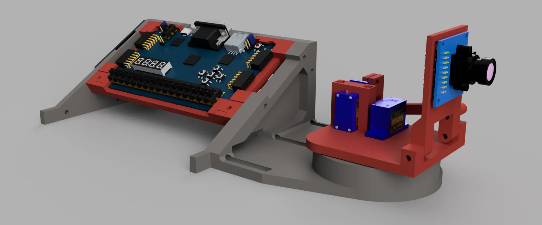
Mechanical Design
For a bit of flair, the FPGA boards and pan-tilt were mounted together with the overall theme being a retro arcade machine.
A simple coin slot with aluminium foil was added to the left side of the mount. With a metal coin, a closed circuit is formed, pulling a digital input pin on the FPGA high, and allowing for a fun way to start the object tracker by literally inserting a coin into the machine.
As for the pan-tilt itself, the shaft of the pan servo is clamped to the base, so the whole pan-tilt assembly rotates when the pan servo moves. The camera plate is also mounted on a hinge and the tilt servo connects to the plate through a simple linkage. While this limits the range of motion along the tilt axis, it made the whole assembly much smaller than what a direct connection would have allowed.
Fun fact: This style of pan-tilt assembly was inspired from the Pixycam pan-tilt kit, which was what I used in my first RoboCupJunior Soccer competition back in 2018. Life truly is nothing but a flat circle.
Conclusion
For all the challenges that programming with a HDL brings, the low-level, parallel nature of it also brought along freedoms that a typical CPU would not have allowed for. For example, instead of fiddling with interrupts or threading, all I had to do was instantiate another hardware module to achieve true parallelism. Additionally, instead of scanning through datasheets and setting registers, I could simply define my own signal interfaces directly.
For the EE2026 course itself, this open-ended project did much of the heavy lifting in terms of making the module fun. The content itself was rather basic, focusing on digital logic alone, and did not cover any FPGA specific concepts. Some theory on the architecture of FPGAs and its key components e.g. LUTs, BRAM, DSP slices, etc., as well as how to work with common scenarios like clock domain crossing or pipelining should have been taught, since it would have made it easier for people to understand how to better design for synthesisability.
Nonetheless, definitely enjoyed the open-ended nature of the project, and looking forward to building more stuff with FPGAs!
← Back to projects